- 您现在的位置:买卖IC网 > Sheet目录307 > ADE7761AARSZ-RL (Analog Devices Inc)IC ENERGY METERING 1PHASE 20SSOP
ADE7761A
OPERATION
V CM
POWER SUPPLY MONITOR
The ADE7761A continuously monitors the power supply (V DD )
with its on-chip, power supply monitor. If the supply is less than
4 V ± 5%, the ADE7761A goes into an inactive state, that is, no
energy is accumulated and the CF, F1, and F2 outputs are
disabled. This is useful to ensure correct device operation at
power-up and during power-down. The power supply monitor
+660mV
GAIN
–660mV
GAIN
V 1A , V 1B
+ V CM
V CM
+ V CM
DIFFERENTIAL INPUT A
±660mV MAX PEAK
COMMON MODE
±100mV MAX
AGND
DIFFERENTIAL INPUT B
±660mV MAX PEAK
V1
V1
V 1A
V 1N
V 1B
has built-in hysteresis and filtering, which provides a high
degree of immunity to false triggering due to noisy supplies.
The power supply and decoupling for the part should be such
that the ripple at V DD does not exceed 5 V ± 5% as specified for
normal operation.
V DD
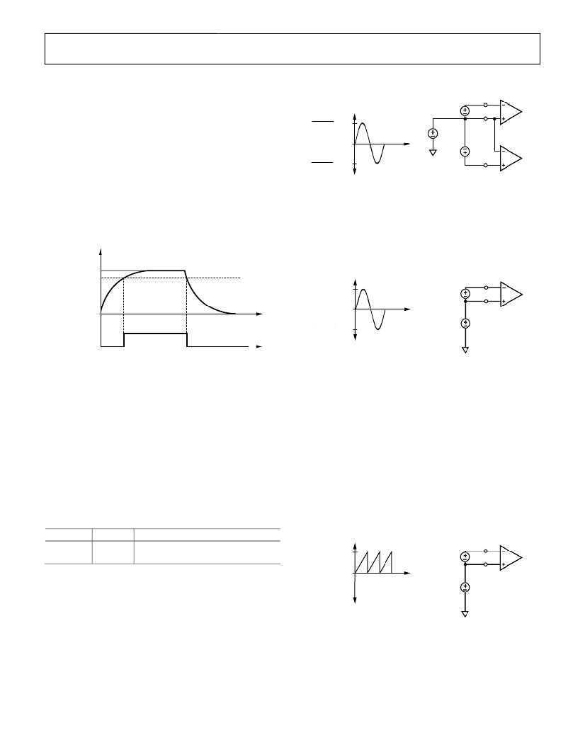
Figure 12. Maximum Signal Levels, Channel 1
Channel V2 (Voltage Channel)
The output of the line voltage transducer is connected to the
ADE7761A at this analog input. Channel V2 is a single-ended,
voltage input. The maximum peak differential signal on Channel 2
is ±660 mV with respect to V 2N . Figure 13 shows the maximum
signal levels that can be connected to Channel 2.
5V
4V
+660mV + V CM
V2
DIFFERENTIAL INPUT
V2
V 2P
0V
V CM
±660mV MAX PEAK
V 2N
ADE7761A
REVP - FAULT - CF - INACTIVE
F1 - F2 OUTPUTS
TIME
ACTIVE
INACTIVE
–660mV + V CM
COMMON MODE
±100mV MAX
V CM
Figure 11. On-Chip, Power Supply Monitoring
ANALOG INPUTS
Channel V1 (Current Channel)
The voltage outputs from the current transducers are connected
to the ADE7761A at Channel V1. It has two voltage inputs, V 1A
and V 1B . These inputs are fully differential with respect to V 1N .
However, at any one time, only one is selected to perform the
power calculation (see the Fault Detection section).
The maximum peak differential signal on V 1A ? V 1N and V 1B ? V 1N
is ±660 mV. However, Channel 1 has a programmable gain
amplifier (PGA) with user-selectable gains of 1 or 16 (see
Table 5). This gain facilitates easy transducer interfacing.
Table 5. Channel 1 Dynamic Range
Figure 13. Maximum Signal Levels, Channel 2
The differential voltage V 2P ? V 2N must be referenced to a
common mode (usually AGND). The analog inputs of the
ADE7761A can be driven with common-mode voltages of up
to 100 mV with respect to AGND. However, the best results
are achieved using a common mode equal to AGND.
MISCAL Input
The input for the power calibration in missing neutral mode
is connected to the ADE7761A at this analog input. MISCAL is
a single-ended, voltage input. It is recommended to use a dc
signal derived from the voltage reference to drive this pin. The
maximum peak differential signal on MISCAL is 660 mV with
respect to V 2N . Figure 14 shows the maximum signal levels that
can be connected to the MISCAL pin.
PGA
0
1
Gain
1
16
Maximum Differential Signal (mV)
660
41
MISCAL
+660mV + V CM
DIFFERENTIAL INPUT
±660mV MAX PEAK
MISCAL
MISCAL
V CM
V 2N
Figure 12 shows the maximum signal levels on V 1A , V 1B , and
V 1N . The maximum differential voltage is ±660 mV divided by
the gain selection. The differential voltage signal on the inputs
must be referenced to a common mode (usually AGND).
COMMON MODE
±100mV MAX
V CM
AGND
Figure 14. Maximum Signal Levels, MISCAL
Rev. 0 | Page 11 of 24
发布紧急采购,3分钟左右您将得到回复。
相关PDF资料
ADE7761BARSZ-RL
IC ENERGY METERING 1PHASE 20SSOP
ADE7768ARZ-RL
IC ENERGY METERING 1PHASE 16SOIC
ADE7769ARZ-RL
IC ENERGY METERING 1PHASE 16SOIC
ADM8843ACPZ-REEL7
IC LED DRVR WHITE BCKLGT 16LFCSP
ADP1653ACPZ-R7
IC LED DRVR PHOTO FLASH 16-LFCSP
ADP1712-EVALZ
BOARD EVALUATION ADP1712
ADP1720-EVALZ
BOARD EVAL FOR ADP1720-ADJ
ADP2140CPZ-REDYKIT
REDYKIT 2 BOARDS ADP2140ACPZ
相关代理商/技术参数
ADE7761ARS
制造商:Rochester Electronics LLC 功能描述: 制造商:Analog Devices 功能描述:
ADE7761ARS-REF
制造商:Analog Devices 功能描述:ENERGY METER IC W/FAULT&MNEUT DETEC. - Bulk
ADE7761ARSRL
制造商:AD 制造商全称:Analog Devices 功能描述:Energy Metering IC with On-Chip Fault and Missing Neutral Detection
ADE7761B
制造商:AD 制造商全称:Analog Devices 功能描述:Energy Metering IC with On-Chip Fault and Missing Neutral Detection
ADE7761BARS
制造商:Rochester Electronics LLC 功能描述: 制造商:Analog Devices 功能描述:
ADE7761BARS-REF
制造商:AD 制造商全称:Analog Devices 功能描述:Energy Metering IC with On-Chip Fault and Missing Neutral Detection
ADE7761BARS-RL
制造商:AD 制造商全称:Analog Devices 功能描述:Energy Metering IC with On-Chip Fault and Missing Neutral Detection
ADE7761BARSZ
功能描述:IC ENERGY METERING 1PHASE 20SSOP RoHS:是 类别:集成电路 (IC) >> PMIC - 能量测量 系列:- 产品培训模块:Lead (SnPb) Finish for COTS
Obsolescence Mitigation Program 标准包装:2,500 系列:*
